

MPINO Series
MPINO-8A8R-S
MPINO-8A8R-S Industrial Arduino Controller
MPINO-8A8R-S is an ATmega128-AU-based industrial Arduino-compatible PLC controller with 8 isolated digital inputs and 8 relay outputs. Onboard RS-485, I²C with Modbus RTU, programmable in the Arduino IDE. DIN-rail mountable for automation, testing, HMI integration and embedded control.
International shipping (EMS) — calculated at checkout by destination & weight
Shipping weight 250 g (per unit)
Ships the next business day (regardless of order time)
Large orders may take 1 extra day to dispatch
Cancel before dispatch · request a return/exchange after delivery
Key features
/ FEATURES- ATmega128-AU core, programmable in the Arduino IDE and MPINO STUDIO2
- 8 opto-isolated digital inputs (NPN/PNP, up to 40 V tolerant)
- 8 relay outputs for AC/DC dry-contact switching
- 4 analog inputs (0–5 V / 4–20 mA / 0–10 V ranges)
- 2 NTC temperature inputs (−40 to +120 °C)
- Industrial communication: RS-485, I²C · Modbus RTU
- DIN-rail 35 mm mountable, isolated field I/O for the factory floor
Specifications
/ SPEC| MCU | ATmega128-AU |
|---|---|
| Power input | DC 12V – 24V |
| Digital inputs | 8 |
| Relay outputs | 8 |
| Analog inputs | 4 |
| Temperature sensor inputs | 2 |
| High-speed pulse inputs | 4 |
| High-speed pulse outputs | 6 |
| RS-485 | 1ch |
| I²C | 1ch |
| Modbus RTU | Yes |
| LS Cnet | Yes |
| Mitsubishi MC | Yes |
| Arduino IDE compatible | Yes |
Software
Arduino IDE / MPINO Studio 2
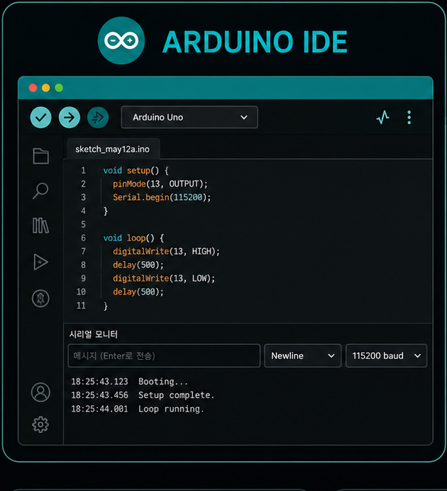
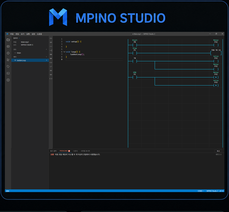

Arduino IDE compatible
Works with the Arduino toolchain you already use

MPINO STUDIO2 included
Arduino code and ladder logic in one tool

Arduino + ladder logic
Build control logic faster with familiar ladder rungs
Setting up the toolchain
Installing the ARDUINO SDK adds this product's board definition to the Arduino IDE and makes the functions that earn their keep in industrial work available as built-in commands. There is no library to add — the Arduino IDE offers them with autocompletion as you type.
Built-in commands the SDK unlocks
- PLC timers · callback timersIton · Itof · Itpl · Itmr · ItimerSet
- CountersIctu · Ictd · Ictud · IgetCount
- Scaling · PID controlIscale · Iscalef · IpidSet · IpidRun
- First-in and last-in buffersFIFO · FILO
- Input debounce · edge detectionIbounce · IdigitalRead · Iup · Idown · Ialt
- Debug · watchdogdebug · debugln · WDT_ENABLE · WDT
- Modbus RTU · LS Cnet · Mitsubishi MCImodbusRTU · ICnet · IMcProtocol
- Analog input · 4–20 mA correctionanalogRead2 · IanalogRead · IanalogFilter · ntcRead
- PWM · pulse · high-speed counterPWM · FDPWM · NPWM · TCNTSETUP · TCNTOUT
Using the Arduino IDE requires the ARDUINO SDK (the ILOGICS board package) to be installed. MPINO STUDIO2 can be used without installing it.
Download CableMP DOWNLOAD CABLE
Programming this board needs the dedicated download cable
The upload port on this board is a mini 5P USB socket, but the USB-to-serial conversion lives in the CABLE, not on the board. Plug in an off-the-shelf mini 5P USB cable and the PC never enumerates a port, so nothing uploads. The MP download cable is one we build ourselves — buy one and keep using it.
USB-TTL converter inside
The conversion IC sits in the connector housing
Generic mini 5P cannot be used
An ordinary cable enumerates no port and cannot upload
USB-A to mini 5P
Connects the PC's USB port to the board's upload port.
Made by ILOGICS
A dedicated cable for use with ILOGICS products.
What the cable is
* Having the conversion IC inside the housing is what sets this apart from an ordinary cable. Board end is mini 5P, PC end is USB-A, and the cable is 1 m long.
Sold separately — order it with the board under Add-on products.
Cable specification
| Item | Detail |
|---|---|
| PC end | USB-A plug |
| Conversion | USB-TTL converter inside the cable |
| Board end | USB mini 5P plug |
| Length | 1 m |
| Driver | FTDI |
Installing the driver
- Connect the MP download cable between the PC's USB port and the board's upload port.
- Open Device Manager and check whether USB Serial Port (COMx) appears under Ports (COM & LPT).
- If it does not appear, install the FTDI driver from the resources section and reconnect the cable.
- In your development tool, select the same COM number Device Manager shows, then upload.
Expansion ConnectorsEXPANSION CONNECTORS
The expansion functions are fitted on Molex 5267-04 4-pin connectors
I²C, PWM, pulse/encoder input and the 7-segment (FND) link are fitted on Molex 5267-04 4-pin connectors, 4 of them on the board. The cables that plug into them are made up with the mating Molex 5264-04 housing, and 4 four-pin cables are included with the board.
4-pin — 5267-04
I²C, PWM, pulse/encoder input and the 7-segment (FND) link
4 on the board
Two PWM headers, one I²C and one ENC/FND — the same 4-pin connector
Mating 5264-04 half
The cable end uses the 5264-04 housing
Cables included
4 four-pin cables ship with the board
Connection diagram
Connector by function
| Function | Board-side connector |
|---|---|
| I²C | Molex 5267-04 (4-pin) |
| PWM output | Molex 5267-04 (4-pin) |
| Pulse / encoder input | Molex 5267-04 (4-pin) |
| 7-segment (FND) | Molex 5267-04 (4-pin) |
Digital input
8 isolated digital input channels
Eight digital input channels read external switches and sensors reliably, straight from the terminal block.
D0–D7 inputs
Eight digital input points in total
COM0 common
All 8 points share COM0
Optocoupler isolation
Control circuit protected from field noise
NPN / PNP sensors
Works with either sensor wiring convention
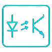

Input channel layout
* Example wiring for external switches or sensors (NPN/PNP shared)
Optocoupler isolation
The digital inputs use a bidirectional optocoupler stage (anti-parallel LEDs), so either NPN or PNP signals are read reliably, with all 8 channels referenced to COM0.
Example sketch — reading an input
// Mirror I(0)~I(7) onto R(32)~R(39)
void setup() {
  for (int k = 32; k <= 39; k++) pinMode(k, OUTPUT);
}

void loop() {
  for (int k = 0; k <= 7; k++) {
    if (digitalRead(k) == HIGH) digitalWrite(32 + k, HIGH);
    else                        digitalWrite(32 + k, LOW);
  }
}
Relay output
8 relay output channels (1a1c)
8 relay output channels control external loads running on AC or DC, reliably.
D32–D39 outputs
8 relay contact output points
8 × 1a1c relays
Each output is an independent relay contact
2 outputs per COM
Each COM terminal is shared by 2 outputs
Electrical isolation
Control and output sides separated by the relay

Output channel layout
* Example wiring for external loads (relay contact output)
Relay output structure
Each relay output is a 1a1c relay that mechanically separates the control side from the output side, with 2 outputs sharing one COM terminal. Being a volt-free contact, it switches both AC and DC loads.
Example sketch — driving a relay output
void setup() {
  pinMode(32, OUTPUT);   // R(32)
}

void loop() {
  digitalWrite(32, HIGH);
  delay(1000);
  digitalWrite(32, LOW);
  delay(1000);
}
Analog inputAnalog Input
4 analog input channels, current or voltage selectable per channel
A0–A3 come out on the same green screw terminal block as the digital inputs, at the board's upper right. Every channel ships as a 0(4)–20 mA current input; pull that channel's header cap and it becomes a DC 0(1)–5 V voltage input, and DC 0–10 V can be requested when ordering.
A0–A3 · 4 channels
Four 10-bit (0–1023) analog input points
0(4)–20 mA by default
Header cap fitted at the factory · 250 Ω input
Cap off → DC 0(1)–5 V
Selected independently per channel · 200 kΩ
External reference
REF3025 +2.5 V on AREF for accurate readings
Analog input terminals
* The same green screw terminal block as the digital inputs, at the board's upper right, in the order A0 · A1 · A2 · A3 · AGND. Each channel has its own 2-pin range-select header, shipped with the cap fitted. AGND is tied to GND through a 2012 0 Ω resistor.
Input range options
| Input range | How it is set | Input resistance |
|---|---|---|
| 0(4)–20 mA | Header cap fitted (factory default) | 250 Ω |
| DC 0(1)–5 V | Header cap removed | 200 kΩ |
| DC 0–10 V | Resistor change + cap removed (on request) | 400 kΩ |
All four channels are 10-bit (0–1023) and reference REF3025 +2.5 V fed to AREF. The range is selected independently per channel.
Example sketch — reading an analog input
unsigned int ADC0;

void setup() {
  Serial.begin(9600);
}

void loop() {
  ADC0 = analogRead(A0);                                 // 0~1023
  ADC0 = ((unsigned long)ADC0 * (3000 - 0)) / 1023 + 0;  // rescale to 0~3000
  Serial.print("A0 = "); Serial.println(ADC0);
  delay(500);
}
Temperature inputNTC Temperature
2 NTC temperature channels on their own connectors
NTEMP1 and NTEMP2 each take an NTC 3950 10 kΩ thermistor and read −40 to 120 °C in 0.1 °C steps. They use their own connectors, separate from the analog inputs, and have no polarity — the two leads are interchangeable.
NTEMP1 · NTEMP2
Two temperature channels on A4 (D52) / A5 (D53)
NTC 3950 10 kΩ
10 kΩ at 25 °C, B constant 3950 K
−40 to 120 °C
0.1 °C resolution (over 0–40 °C)
Own JST XH connectors
2.54 mm 2-pin × 2 · no polarity
NTC temperature connectors
* Two white JST XH 2-pin connectors (2.54 mm pitch) — 2 pins per channel, 4 pins for both. The NTC input has no polarity, so the two leads are interchangeable.
Temperature sensor specs
| Sensor | NTC 3950 K · 10 kΩ at 25 °C |
|---|---|
| Channels | NTEMP1 = A4 (D52) · NTEMP2 = A5 (D53) |
| Measuring range | −40 to 120 °C |
| Resolution | 0.1 °C (over 0–40 °C) |
| Connector | White JST XH 2-pin (2.54 mm) × 2 · no polarity |
| Reading | ntcRead() returns tenths of a degree (251 → 25.1 °C) |
A4 / A5 share the ADC — and therefore the same reference — with the analog inputs.
Example sketch — reading the NTC temperature
unsigned int Temp;

void setup() {
  Serial.begin(9600);
}

void loop() {
  Temp = ntcRead(analogRead(A4));   // A4 = NTEMP1 (A5 = NTEMP2)
  Serial.print("Temp = "); Serial.print(Temp / 10.0, 1); Serial.println(" C");
  delay(500);
}

int ntcRead(unsigned int RawADC) {
  float v;
  v = (1023.0F / (float)RawADC) - 1.0F;
  v = 10000.0F / v;
  float steinhart;
  steinhart  = v / 10000.0F;
  steinhart  = log(steinhart);
  steinhart /= 3950.0F;                       // NTC B constant (10K 3950)
  steinhart += 1.0F / (25.0F + 273.15F);
  steinhart  = 1.0F / steinhart;
  steinhart -= 273.15F;
  return (unsigned int)(steinhart * 10);      // 0.1 C units
}
High-speed pulse outputPWM Output
6 PWM output points on two 4-pin headers, driven by two timers
D21, D22, D23 (Timer3) and D26, D27, D28 (Timer1) come out on two 4-pin headers under one PWM silkscreen — three outputs plus a GND on each. The output swings LOW DC 0 V to HIGH DC 5 V at up to 30 mA per point, and analogWrite() takes a duty of 0–255 that extends to 0–65535 once the timer registers are changed.
6 PWM points
Two 4-pin headers · three outputs + GND on each
Two timer groups
D21–D23 = Timer3 · D26–D28 = Timer1
8-bit → 16-bit duty
0–255 by default, 0–65535 after the register change
DC 5 V · 30 mA
LOW 0 V / HIGH 5 V · up to 30 mA per point
Timer assignment per pin
| Pin | Timer channel | Note |
|---|---|---|
| D21 | Timer3 A | Shares Timer3 with the counter mode |
| D22 | Timer3 B | Shares Timer3 with the counter mode |
| D23 | Timer3 C | Shares Timer3 with the counter mode |
| D26 | Timer1 A | — |
| D27 | Timer1 B | — |
| D28 | Timer1 C | — |
The output is LOW DC 0 V / HIGH DC 5 V at up to 30 mA. Duty is set with analogWrite(pin, value) over 0–255; for 16-bit duty, set TCCR3A=0xAA; TCCR3B=0x1A; ICR3=65535; in setup() for D21–D23.
Pulse output headers and duty
* Two 4-pin headers at the board's centre, under a single PWM silkscreen that spans both. The left header is 21 · 22 · 23 · GND and the right one 26 · 27 · 28 · GND, each with its own GND pin, and the numbers on the board are the pin numbers used in code. The two headers are driven by different timers, so the timer a pin belongs to decides which pins can change together.
Before you wire it
- D21, D22 and D23 run on Timer3, the same resource the hardware high-speed counter uses. While the counter is running in that mode these three cannot output PWM — use D26, D27 and D28 instead.
- analogWrite() works on these six pins only. It has no effect on any other pin.
- Writing Timer1 or Timer3 registers directly affects every PWM pin that timer drives, not just the one you are changing.
- Each point supplies up to 30 mA. Drive a larger load through the transistor or relay outputs, or through an external driver.
Example sketch — PWM output
void setup() {
  // PWM is available on D21~D23 and D26~D28 only
}

void loop() {
  if (digitalRead(0) == HIGH) analogWrite(21, 127);   // 50% duty
  else                        analogWrite(21, 0);
}
External interruptInterrupt
Count high-speed pulses and read a rotary encoder from the interrupt inputs
CLK (D24), DIO (D25), SCL (D18) and SDA (D19) are the four interrupt inputs, with a built-in pull-up on each — 4.7 kΩ on SCL and SDA, 10 kΩ on CLK and DIO. attachInterrupt() catches the edge, so the same inputs count high-speed pulses or read a rotary encoder's rotation and direction, at 50 kHz and above. The counter also has a hardware mode that runs Timer3 straight off the CLK input.
4 interrupt inputs
CLK (D24) · DIO (D25) · SCL (D18) · SDA (D19)
High-speed pulse counting
In the ISR, or in Timer3 counter mode · 50 kHz and above
Rotary encoder input
Open-collector on SCL / SDA, totem-pole on CLK / DIO
Pull-ups built in
SCL · SDA 4.7 kΩ, CLK · DIO 10 kΩ · DC 0–5 V · HIGH from 3 V
Interrupt pin mapping
| Pin | INT | Built-in resistor · shared with |
|---|---|---|
| D18 | INT0 | 4.7 kΩ pull-up · I²C SCL |
| D19 | INT1 | 4.7 kΩ pull-up · I²C SDA |
| D24 | INT6 | 10 kΩ pull-up · CLK · FND / encoder |
| D25 | INT7 | 10 kΩ pull-up · DIO · FND / encoder |
Input is DC 0–5 V, with HIGH recognised from 3 V, and at least 50 kHz. If a pin is used as an interrupt, the function sharing it (I²C, FND) cannot be used. High-speed counting works two ways: attachInterrupt() adds to a variable in the ISR, or Timer3 is put into counter mode and counts the CLK input in hardware — that second mode uses the same resource as pulse outputs D21–D23, so the two cannot run together. The frequency actually handled in the ISR depends on the length of that routine and the load of the whole program, so it is not guaranteed as a fixed figure.
What the interrupts are for
* On the left the pulse source's output goes to the CLK terminal and its ground to GND, and every rising edge adds one in the interrupt service routine. On the right the encoder's two phases sit 90° apart, so the level of DIO at a rising CLK edge is the direction of rotation.
Interrupt connectors
* Two 4-pin connectors on the board's left edge, drawn in the order the pins are silkscreened. CLK is D24 (INT6), DIO is D25 (INT7), SCL is D18 (INT0) and SDA is D19 (INT1). The FND (7-segment) accessory and I²C use the same pins, so they cannot be used if those pins serve as interrupts.
Before you wire it
- The interrupt inputs accept DC 0–5 V only. Connecting a 24 V signal directly will destroy the MCU.
- These four pins are the only interrupt inputs. D30 and D31 belong to the RS-485 port and must never be used as interrupts or as general-purpose I/O.
- An encoder goes on different terminals depending on its output stage: open-collector on SCL (D18) and SDA (D19), totem-pole or push-pull on CLK (D24) and DIO (D25).
- Using D24 and D25 as interrupts means the FND (7-segment) accessory on the same connector cannot be used at the same time.
- Using D18 and D19 as interrupts means I²C cannot be used at the same time.
- Counting in Timer3 counter mode shares its resource with the pulse outputs D21–D23, so the two cannot be used together — move PWM to D26–D28.
- Inside the ISR, only increment the count — do not call Serial, delay() or floating-point maths.
- Changing the built-in resistor configuration on CLK and DIO is SMD rework. Please ask us rather than modifying the board yourself.
Example sketch — pulse counting (interrupt)
unsigned int count = 0;

void setup() {
  Serial.begin(9600);
  attachInterrupt(digitalPinToInterrupt(CLK), countFunc, RISING);
}

void loop() {
  Serial.println(count);
}

void countFunc() { count++; }
Example sketch — rotary encoder
volatile long encoderValue = 0;

void setup() {
  Serial.begin(115200);
  attachInterrupt(digitalPinToInterrupt(CLK), updateEncoder, RISING);
}

void loop() {
  Serial.print("Encoder: ");
  Serial.println(encoderValue);
  delay(500);
}

void updateEncoder() {
  if (digitalRead(DIO)) { encoderValue++; }
  else { encoderValue--; }
}
Example sketch — counting in Timer3 counter mode
unsigned int HCNT3;

void setup() {
  TIMSK  = 0x00;
  TCCR3A = 0x00;
  TCCR3B = 0x07;
  TCNT3  = 0x00;
}

void loop() {
  HCNT3 = TCNT3;
}

void hcntReset() {
  TCNT3 = 0;
}CommunicationRS-485 · I²C
RS-485, I²C and a USB serial port
RS-485 is Serial1, brought out on a screw terminal as 485+ and 485− for a 1:N multidrop bus, and Modbus RTU works as either master or slave. I²C brings its own 4.7 kΩ pull-ups for a DS3231 RTC or a character LCD, and the USB port handles program upload and debugging.
RS-485 · 1 channel
Serial1 · 1:N multidrop on the 485+ / 485− terminals
Modbus RTU
Works as master or slave
I²C · 1 channel
4.7 kΩ pull-ups built in · 1:N · RTC, character LCD
USB serial
Upload and debug over the USB port
I²C · USB connectors
* The I²C connector is silkscreened I2C and reads SCL · SDA · +5V · GND from the pin-1 end; it doubles as an interrupt and encoder input. The program upload port is the mini USB-B connector at the board's right edge.
RS-485 link
* The 4-pole screw block standing at the board's right edge, in the order 485+ · 485− · GND · +5V from the top. RS-485 is a multidrop bus, so 485+ goes to every node's 485+ and 485− to every node's 485−. To reach RS-232 or UART instead, use the converter module sold separately.
Communication ports
| Port | Pins | Use |
|---|---|---|
| Serial | D16 · D17 | Program upload and debug over the USB port |
| Serial1 | D30 (RX1) · D31 (TX1) | RS-485 on the 485+ / 485− terminals · 1:N |
| Wire (I²C) | SCL = D18 · SDA = D19 | 4-pin connector · 4.7 kΩ pull-ups built in |
RS-485 is reached as Serial1 and supports 1:N multidrop with a MAX485 transceiver carrying ±15 kV HBM ESD protection; Modbus RTU works as either master or slave. I²C also supports 1:N and takes accessories such as the DS3231 RTC and 1602 / 2004 character LCDs. This board has no Serial2 or Serial3.
Before you wire it
- D30 and D31 belong to Serial1 / RS-485. Never reuse them as interrupts or as general-purpose I/O.
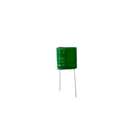
- The +5V pole of the RS-485 block is a supply OUTPUT rated 1 A or less, and can also be used to feed the board 5 V; a supercapacitor connected there holds the internal 5 V up through a power cut — see Power · Data retention below.
- Using D18 and D19 as external interrupts means I²C cannot be used at the same time.
- Uploading requires the MP download cable, which has the USB-TTL converter built in. An off-the-shelf mini 5P cable cannot upload.
- To reach RS-232 or UART, use the separately-sold converter module rather than changing the transceiver in the field.
- This board has no Serial2 or Serial3 — only Serial and Serial1 exist.
Example sketch — serial send and receive
void setup() {
  Serial.begin(9600);
  Serial1.begin(9600);   // RS-485 - Modbus RTU starts the same way
}

void loop() {
  if (Serial1.available()) {
    int b = Serial1.read();
    Serial.write(b);       // RS-485 -> download port
  }
  if (Serial.available()) {
    int b = Serial.read();
    Serial1.write(b);
  }
}
Display connectionLCD · FND
Show status on a character LCD or a 7-segment display — four wires either way
A character LCD goes on the I²C 4-pin connector and a 7-segment (FND) display on the ENC/FND 4-pin connector. Both connectors bring out +5V and GND beside the two signal lines, so the whole run is four wires, and the I²C pull-ups are already on the board.
Character LCD 1602 · 2004
16 × 2 or 20 × 4 characters over I²C
7-segment (FND)
CLK and DIO on the ENC/FND connector · up to 4
4.7 kΩ pull-ups built in
No external resistors to add for I²C
1:N on I²C
Shares the bus with accessories such as the DS3231 RTC
Character LCD on I²C
* The I²C connector is silkscreened I2C and reads SCL · SDA · +5V · GND. SDA is D19 and SCL is D18, both with a 4.7 kΩ pull-up on the board. The 1602 shows 16 characters over 2 lines and the 2004 shows 20 over 4. For a richer display than a character LCD, a touch HMI connects over the serial port instead.
7-segment (FND) on ENC/FND
* The connector is silkscreened ENC/FND and reads CLK · DIO · GND · +5V. CLK is D24 and DIO is D25. One display goes on this connector, and using the PWM headers as well takes the total to 4. The display comes in a decimal-point form and a time-displaying form.
Before you wire it
- Using D18 and D19 as external interrupts means I²C — and with it the character LCD — cannot be used at the same time.
- Using D24 and D25 as external interrupts or as an encoder input means the 7-segment (FND) display cannot be used at the same time.
- The signal pins on both connectors are DC 0–5 V inputs. Applying more than 5 V destroys the MCU.
- The character LCD and the 7-segment display are accessories sold separately — neither is included with the board.
Displays and their connectors
| Display | Connector | Signals |
|---|---|---|
| Character LCD 1602 | I²C 4-pin | 16 characters × 2 lines · SDA = D19 · SCL = D18 |
| Character LCD 2004 | I²C 4-pin | 20 characters × 4 lines · SDA = D19 · SCL = D18 |
| 7-segment (FND) | ENC/FND 4-pin | CLK = D24 · DIO = D25 |
| I²C pull-ups | On the board | 4.7 kΩ · 1:N connection supported |
Both connectors carry +5V and GND alongside the two signal lines, so a display needs no supply of its own. I²C has its 4.7 kΩ pull-ups fitted on the board and supports 1:N, so a character LCD can share the bus with another I²C accessory such as the DS3231 RTC. Character LCDs and 7-segment displays are sold separately.
Example sketch — talking to an I²C device
#include <Wire.h>

void setup() {
  Wire.begin();          // D18 = SCL, D19 = SDA, 4.7k pull-ups on the board
  Serial.begin(9600);
}

void loop() {
  for (uint8_t addr = 1; addr < 127; addr++) {   // scan the bus
    Wire.beginTransmission(addr);
    if (Wire.endTransmission() == 0) {
      Serial.print("Found 0x"); Serial.println(addr, HEX);
    }
  }
  delay(2000);
}
Power · Data retentionPower · Backup
DC 12V ~ 24V in, 5 V out — and your data survives the blackout
The controller takes DC 12V ~ 24V and converts it to 5 V internally with a LM2576 + TPS5430 regulator. Size the supply for at least 24V 0.5A.
DC 12V ~ 24V
Size the supply for 24V 0.5A or more
5 V internal
LM2576 + TPS5430 DC-DC conversion
+5 V out 1A
From the +5 V pole of the RS-485 terminal block
Supercapacitor hold-up
About ten seconds on the +5 V pole
Before wiring the supply
- EEPROM cells last about 100,000 writes. Keep fast-changing values in RAM and write them only when the mains drops — see the two methods below — not every loop.
- USB power is for development and bench testing. Apply the external supply for field installation.
Where the power goes
* Either source runs the board: the external supply through the regulator, or the download port's 5 V directly. The supercapacitor sits on the same 5 V node and keeps it alive when both go away.
Power and data retention
| Input voltage | DC 12V ~ 24V |
|---|---|
| Recommended supply | 24V 0.5A or more |
| Internal conversion | LM2576 + TPS5430 DC-DC to 5 V |
| +5 V output | 1A max, from the +5 V pole of the RS-485 terminal block |
| USB-powered operation | Runs on the PC's 5 V through the download port |
| Non-volatile memory | EEPROM 4 KB, about 100,000 writes |
| Hold-up on a power cut | Supercapacitor on the +5 V pole, about ten seconds |
| Blackouts retained | More than 100,000, writing only when the mains drops |
Size the supply for 24V 0.5A or more, plus whatever the +5 V pole is feeding (up to 1A).
Two ways to keep data through a blackout
Which one you want depends on how often the value changes. They are meant to be combined.
EEPROM — values that change occasionally
The on-board EEPROM holds 4 KB with no power at all and is written a byte at a time, but the same cell survives only about 100,000 writes. That makes it right for setpoints, calibration data and machine configuration — and wrong for anything the loop updates.
Supercapacitor — values that change constantly
Fit a supercapacitor to the +5 V pole and the internal 5 V stays up for about ten seconds after the main supply is cut. Wire the main supply into a digital input, and the moment digitalRead() sees that input go off, write the value to EEPROM; when power comes back, setup() reads the stored value out of EEPROM and puts it into memory. Because the EEPROM is written only at the instant of a blackout, it survives more than 100,000 of them.
MPINO STUDIO2 — done for you
MPINO STUDIO2 offers supercapacitor-based retention as an option, so the sequence above can be set up in the tool instead of being coded by hand.
Mounting · DIN railDIN Rail
Clips onto a 35 mm DIN rail, or screws down through the PCB's own holes
Inside a control panel the board clips onto a 35 mm DIN rail; built into a machine it screws down through the Ø3.2 mounting holes in the PCB. The board measures 95.8 × 100.0 mm without the rail clip, and stands 114.2 mm high once the clip is closed on the rail.
35 mm DIN rail
Clips onto the rail in a control panel
Direct PCB mounting
Screws through the Ø3.2 mounting holes
95.8 × 100.0 mm
PCB outline with no rail clip fitted
114.2 mm engaged
119.4 mm with the clip open, 114.2 mm closed
Mounting and dimensions
| Mounting | 35 mm DIN rail, or direct to PCB (Ø3.2 holes) |
|---|---|
| DIN rail | 35 mm |
| PCB alone (no clip) | 95.8 × 100.0 mm |
| Mounting holes | Ø3.2 mm · 79.0 × 90.0 mm apart |
| Clip open (before engaging) | approx. 119.4 mm |
| Clip closed (engaged) | approx. 114.2 mm |
Where no DIN rail is used, the board screws down through the Ø3.2 mounting holes in the PCB; on a rail, the clip closes over a 35 mm profile and the assembly stands 114.2 mm high.
Mounting on a 35 mm DIN rail
* The clip hooks over a 35 mm DIN rail. Overall height is 119.4 mm with the clip open and 114.2 mm once it is closed and engaged. The drawing shows the mounting method rather than the clip's own shape.
Outline and mounting holes
* The outline and mounting holes with no rail clip fitted. All dimensions in millimetres.
Installation notes
- Indoor use only. Do not install where there is rain, dust, frost, direct sunlight or condensation.
- Do not install in an atmosphere containing flammable or explosive gas.
- Do not install where there is heavy vibration or shock.
- Where the equipment affects life or property (nuclear, medical, marine, vehicle, aviation and the like), a secondary safety device must be fitted.
FAQ
How many I/O points does the MPINO-8A8R-S have?▾
The MPINO-8A8R-S provides 8 isolated digital inputs and 8 relay outputs, with onboard RS-485, I²C communication. See the specification table for the full breakdown.
Does the MPINO-8A8R-S support Modbus RTU?▾
Yes. The MPINO-8A8R-S supports Modbus RTU — master and slave alike — over its serial interface.
Related controllers
/ RELATED


Related guides
/ DOCSModbus RTU on Industrial Arduino: A Practical Guide
Wire RS-485, run a Modbus RTU master and slave on MPINO controllers with the SDK's built-in command set, and integrate with HMIs and SCADA.
RS-485 Networking for Industrial Arduino Controllers
Multi-drop wiring, termination, biasing, and automatic direction control for reliable RS-485 field buses.
How to Connect an HMI to an Industrial Arduino
Expose live I/O and process values to a touchscreen HMI over Modbus RTU or I²C, with register mapping examples.