

MPS Series
MPS-16A8R8T
MPS-16A8R8T Industrial PLC Controller
MPS-16A8R8T is an industrial PLC controller with 16 isolated digital inputs and 16 relay + transistor outputs. Onboard RS-232, RS-485, UART, I²C, programmed in MP STUDIO ladder logic. DIN-rail mountable for automation, testing, HMI integration and machine control.
International shipping (EMS) — calculated at checkout by destination & weight
Shipping weight 350 g (per unit)
Ships the next business day (regardless of order time)
Large orders may take 1 extra day to dispatch
Cancel before dispatch · request a return/exchange after delivery
Key features
/ FEATURES- Programmed in MP STUDIO ladder logic
- 16 opto-isolated digital inputs (NPN/PNP, up to 40 V tolerant)
- 8 relay outputs for AC/DC dry-contact switching
- 8 transistor (sink) outputs for fast DC switching
- 4 analog inputs (0–5 V / 4–20 mA / 0–10 V ranges)
- 2 analog outputs
- 2 NTC temperature inputs (−40 to +120 °C)
- Industrial communication: RS-485, RS-232, UART, I²C · Modbus RTU
- DIN-rail 35 mm mountable, isolated field I/O for the factory floor
Specifications
/ SPEC| Power input | DC 12V – 24V |
|---|---|
| Digital inputs | 16 |
| Relay outputs | 8 |
| Transistor outputs | 8 |
| Analog inputs | 4 |
| Analog outputs | 2 |
| Temperature sensor inputs | 2 |
| High-speed pulse inputs | 2 |
| High-speed pulse outputs | 4 |
| Encoder inputs | 1 |
| RS-232 | 1ch |
| RS-485 | 1ch |
| UART | 1ch |
| I²C | 1ch |
| Modbus RTU | Yes |
| LS Cnet | Yes |
Software
MP STUDIO — Ladder Logic
The MPS series is programmed in MP STUDIO, a free ladder-logic IDE. Draw the control logic as a ladder diagram and call analog, temperature, high-speed counter and pulse output straight from function blocks.
Ladder logic only
Contacts and coils — existing PLC experience transfers directly
Function blocks
ADC · NTEMP · HCNT · ENCODER · PWM, each a single block
Live monitoring
Ctrl+T to download, Ctrl+M to monitor and debug on the machine
Before the first download
Install MP STUDIO from the ILOGICS download centre, pick your model in the device list, set the COM port, and you can download straight away.
Models that use the MP download cable appear in Device Manager as "USB Serial Port". If it does not appear, install the FTDI driver as well.
Digital input
16 isolated digital input channels
16 digital input channels read external switches and sensors straight from the terminal block. In the ladder program they are the contacts P0–P15.
P0–P15 inputs
16 isolated digital input points in total
COM0 / COM1 commons
COM0 = P0–P7 · COM1 = P8–P15 (8 points per COM)
DC 0–40 V input
DC 5 V and above reads as HIGH · optocoupler isolated
NPN / PNP sensors
Either sensor wiring convention is read as-is

Input channel layout
* Example wiring for external switches or sensors — applying DC 12–24 V at the terminal turns that contact memory ON
Optocoupler isolation
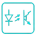
The digital inputs use a bidirectional optocoupler stage — anti-parallel LEDs into a phototransistor — so either NPN or PNP wiring is read, and the field side stays electrically separate from the control circuit.
Example ladder — reading an input
        P0                                  P32
0000  --| |---------------------------------( )--

  P0 = push button (digital input), P32 = lamp on the transistor (sink) output.
  P0 ON  -> P32 ON        P0 OFF -> P32 OFF
  The sixteen inputs return to two commons: P0~P7 to COM0 and P8~P15 to COM1.
Transistor output
8 non-isolated sinking transistor output channels
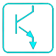
8 transistor output channels switch external loads. When the ladder turns one of the output contacts P32–P39 on, that terminal is driven to GND — a sinking output.
P32–P39 outputs
8 non-isolated sinking transistor output points
V+ / GND supply
Connect the load supply's P(+) to V+ and its N(−) to GND
Non-isolated sinking output
The output's reference potential is the board's own GND
Sinking output, 1 A
Up to 1 A per point · up to 6 A across all 8 points
Output channel layout
* Example wiring for external loads — the load goes between V+ and the output terminal. ⚠️ Applying a P(+) voltage to an output terminal while that output is ON shorts it and destroys the transistor.
Output stage structure
This output stage is not isolated. The MCU drives the N-MOSFET gate directly through a driver stage, and the current at the output terminal — up to 1 A per point — is carried by that MOSFET, whose drain is the output terminal and whose source ties to the board's own GND. The load supply's negative therefore shares the board GND.
Example ladder — driving a transistor output
        P1                                  P33
0000  --| |---------------------------------(S)--

        P2                                  P33
0001  --| |---------------------------------(R)--

        P3                                  P32
0002  --| |---------------------------------(S)--

  P1 = start button, P2 = stop button, P33 = a lamp on the transistor output.
  P1 ON latches P33 on (it stays on when P1 is released); P2 ON clears it.
  Turning a transistor output ON connects GND to that terminal; OFF leaves it floating,
  so the load hangs between V+ and the terminal.
Relay output
8 isolated relay output channels, volt-free contacts
8 relay output channels switch external loads. Turning one of the output contacts P40–P47 on in the ladder closes that contact onto its COM — a volt-free contact, so it takes DC and AC loads alike.
P40–P47 outputs
8 isolated relay output points
COM3 / COM4 / COM5 / COM6 commons
COM3 = P40–P41 · COM4 = P42–P43 · COM5 = P44–P45 · COM6 = P46–P47 (2 points per COM)
DC or AC loads
0–30 V D.C / 0–250 V A.C volt-free contact
Rated 5 A
Up to 5 A per point
Output channel layout
* Example wiring for external loads — the load supply comes in on the COM side. The relay contact is volt-free, so it may switch DC of either polarity or AC. The contact is rated 0–30 V D.C / 0–250 V A.C, up to 5 a per point.
Relay output stage
The control circuit drives the relay coil, and the load is switched by a contact that is electrically separate from that coil. The contact carries no voltage of its own, so neither the type nor the polarity of the load supply matters.
Example ladder — driving a relay output
        P0                                  P40
0000  --| |---------------------------------( )--

  P0 = push button (digital input), P40 = motor on the relay output.
  When the P40 memory turns ON the relay terminal is physically connected to its COM.
  The eight relay points are grouped two to a common: P40 P41 on COM3, P42 P43 on COM4,
  P44 P45 on COM5 and P46 P47 on COM6.
Analog inputAnalog Input
4 analog input channels on a screw block — the range is selected on the board
AI0–AI3 and AGND come out on one screw block. All 4 channels are 10-bit, and the input range is set on the board itself: 3 ranges, whose setting method is in the table below. The ladder reads a channel with the ADC function block.
AI0–AI3 · 4 channels
4 analog input points, 10-bit (0–1023)
3 selectable ranges
0(4)–20 mA · DC 0(1)–5 V · DC 0–10 V
Set on the board
The header cap picks the range — no wiring change
ADC2 for 4–20 mA
A current or 1–5 V sensor reads 0–818
Analog input terminal
* The screw block reads AI0 · AI1 · AI2 · AI3 and AGND. The range is chosen by the header beside it, and the same choice applies to the channels wired through it — check it before wiring a sensor.
Input ranges and how to select them
| Range | How it is selected | Input resistance |
|---|---|---|
| 0(4)–20 mA | Factory default — the jumper cap is fitted | 250 Ω |
| DC 0(1)–5 V | Remove the jumper cap | 1 MΩ |
| DC 0–10 V | Listed as Optional only | 2 MΩ |
Every channel is 10-bit (0–1023) and is read with the ADC function block. A 4–20 mA or DC 1–5 V sensor must be read with ADC2 instead, and its span is 0–818 rather than 0–1023.
Example ladder — reading an analog input
        @ON               ADC
0000  --| |---------------[ CHANNEL:0 | MAX VALUE:1000 | MIN VALUE:0 | OUT:D0 ]--

  Channel AI0 arrives in D0 as 0~1000. The input range is chosen by the jumper cap on
  the board, and it ships fitted at 0(4)~20mA. For 4~20mA or DC 1~5V use ADC2 instead,
  whose span is 0~818 rather than 0~1023.
Temperature inputNTC
2 NTC temperature channels on a terminal block of their own
2 NTC temperature channels, T0 · T1, on a terminal block of their own with a shared AGND pole — separate from the analog input block. The ladder reads one with the NTEMP function block, which returns tenths of a degree — 234 means 23.4℃.
2 NTC channels
T0 · T1
-40℃ to 120℃
Measuring range, resolution 0.1℃
NTEMP function block
CHANNEL and OUT — a reading of 234 is 23.4℃
NTC 3950K 10KΩ(25℃)
Thermistor this input is scaled for
NTC terminals
* Both channels sit on one terminal block and share the AGND pole. The input is scaled for a NTC 3950K 10KΩ(25℃) thermistor; a 10KΩ pull-up is fitted on the board and the divider hangs off the 2.5 V reference and reaches the MCU through a low-pass filter.
Temperature input specs
| Channels | 2 points · T0 · T1 |
|---|---|
| Sensor | NTC 3950K 10KΩ(25℃) |
| Measuring range | -40℃ to 120℃ |
| Resolution | 0.1℃ (over 0–40℃) |
| Pull-up resistor | 10KΩ |
| Function block | NTEMP (CHANNEL / OUT) |
NTEMP returns the temperature in tenths of a degree: read T1 and a value of 234 means 23.4℃.
Example ladder — reading the NTC temperature
        @ON               NTEMP
0000  --| |---------------[ CHANNEL:1 | OUT:D10 ]--

  NTEMP channel 1 is the T1 terminal, and it lands in D10 in tenths of a degree:
  234 means 23.4 C. T0 and T1 share one AGND pole on the same terminal block.
Analog outputAnalog Output
2 analog output channels — DC 0–5 V at 16-bit resolution
AO0–AO1 come out on a screw block along the board's left edge. The ladder writes a number with the DAC function block and the converter turns it into a voltage — 16 bits across 0–65535, which is the finest resolution anywhere in this series. DC 0–10 V is available as a factory change.
AO0–AO1 · 2 channels
DC 0–5 V analog output
16-bit resolution
0–65535 across the full range
DAC function block
Written straight from the ladder — no library
External supply required
Nothing comes out on USB 5V alone
How the output is produced
* A screw block on the board's left edge, reading AO0 then AO1. The manual publishes no ground pole for this block — take the reference potential from the board's own ground terminals (AGND · GND).
Analog output specs
| Contacts | AO0 · AO1 |
|---|---|
| Points | 2 points, non-isolated |
| Output voltage | DC 0–5 V |
| Option | DC 0–10 V |
| Resolution | 16-bit (0–65535) |
| Function block | DAC — CHANNEL 0–1 / MAX VALUE / MIN VALUE / OUT |
Example from the manual: with MAX VALUE 1,000 and OUT 500 on channel 0, half the range is requested, so 2.5 V appears at the terminal.
Before you wire it
- The analog output cannot be used while the board runs on USB 5V alone. Connect the external DC 12 V–24 V supply.
- DC 0–10 V is a resistor change made before the board ships — ask for it when you order. It cannot be changed in the field.
- This block has no ground pole of its own. Take the reference potential from the board's ground terminals (AGND · GND).
- This output is not isolated.
Example ladder — driving an analog output
        @ON               DAC
0000  --| |---------------[ CHANNEL:0 | MAX VALUE:1000 | MIN VALUE:0 | OUT:500 ]--

  Channel 0 is the AO0 terminal. MAX VALUE 1000 spans the whole DC 0~5V output, so
  OUT:500 asks for half of it and 2.5V appears at the terminal.
  The output stays at 0V while the board runs on USB 5V alone - connect the external
  DC 12V~24V supply before you expect a reading.
High-speed pulse outputPWM Output
4 PWM output points on 2 independent timers
PWM0–PWM4 are 4 pulse outputs driven by 2 timer resources — channel 0 = PWM0–PWM1 · channel 1 = PWM3–PWM4. Ports on the SAME timer share a WIDTH and a frequency; the two groups are independent of each other, so this board can emit two different frequencies at once. The output swings DC 0 V LOW to DC 5 V HIGH at up to 30 mA per point.
4 PWM points
PWM0–PWM4 · DC 0 V / DC 5 V output
2 timers
channel 0 = PWM0–PWM1 · channel 1 = PWM3–PWM4
DUTY / WIDTH 0–65535
Set the pulse directly, or give a frequency instead
DC 5 V · 30 mA
LOW DC 0 V / HIGH DC 5 V · up to 30 mA per point
Pulse output header and duty
* 2 headers, silkscreened PWM0 · PWM1 · GND / PWM3 · PWM4 · GND. channel 0 = PWM0–PWM1 · channel 1 = PWM3–PWM4.
Before you wire it
- PWM0, PWM1 run on channel 0: they must all carry the same WIDTH and the same frequency — changing one changes the group.
- PWM3, PWM4 run on channel 1: they must all carry the same WIDTH and the same frequency — changing one changes the group.
- The two groups are independent, so they may run at different frequencies at the same time.
- FPWM, NPWM set their timer's CLOCK and WIDTH themselves to hit the frequency you ask for, so mixing them with the PWM block on the SAME timer is not recommended. Driving one timer with PWM and the other with FPWM / NPWM is fine.
- DUTY may not exceed WIDTH. The smaller the WIDTH, the higher the output frequency.
- NPWM takes 0–60 kHz, and 30 kHz or below is recommended.
- The manual prints the function blocks' PORT parameter range as 0–5, but this board brings out 4 pulse outputs — PWM0 · PWM1 · PWM3 · PWM4. There is no terminal for the remaining numbers.
Pulse function blocks
| Function block | What it does | Parameters |
|---|---|---|
| PWM | Pulse by duty and width | PORT 0–5 / DUTY 0–65535 / WIDTH 0–65535 |
| FPWM | Pulse by frequency (50% duty) | PORT 0–5 / FREQ 0–1 MHz |
| NPWM | Emit a set number of pulses | PORT 0–5 / FREQ 0–60 kHz / N |
| POFF | Stop the pulse output | PORT |
The output is LOW DC 0 V / HIGH DC 5 V at up to 30 mA per point. channel 0 = PWM0–PWM1 · channel 1 = PWM3–PWM4 — WIDTH and frequency have to match WITHIN a group, and the two groups are free of each other. Whether a port is currently emitting is readable from the special memory @PWM0, @PWM1, @PWM3, @PWM4.
Example ladder — PWM output
        P0                        PWM
0000  --| |-----------------------[ PORT:0 | DUTY:500 | WIDTH:1000 ]--

        P1                        POFF
0001  --| |-----------------------[ PORT:0 ]--

        P0                        FPWM
0002  --| |-----------------------[ PORT:1 | FREQ:1000 ]--

        P0                        NPWM
0003  --| |-----------------------[ PORT:4 | FREQ:2000 | N:100 ]--

  PWM sets the pulse directly; FPWM emits a 50% duty at the frequency asked for, and
  NPWM emits a fixed number of pulses (here 100 at 2kHz on PWM4). PWM0 and PWM1 are the
  0 channel and PWM3 and PWM4 the 1 channel, so WIDTH has to match inside a channel -
  the two channels are free of each other. NPWM allows one on 0,1 and one on 3,4.
High-speed counter · encoderCounter · Encoder
2 isolated counter points up to 5KHz, plus one encoder channel
The two counter points are OPTOCOUPLED — they take DC 0–80 V straight off a field device on their own common COM2. The encoder is a separate, non-isolated channel on the I2C pair, and it doubles as counter channel 2 for open-collector pulse sources. The ladder reads both with the HCNT and ENCODER function blocks.
2 isolated counter points
H0 · H1, returning to their own common COM2
Encoder A and B phases
SDA is the A phase and SCL the B phase — B lagging A counts up
4.7 kΩ pull-up on the encoder pair
Built into the I2C lines — no external resistors
DC 0–80 V · 5KHz
HIGH from DC 5 V or above
What the two kinds of input are for
* The counter poles are isolated: a 24V pulse source connects straight to H0 · H1 with its return on COM2, and HIGH is recognised from DC 5 V or above. The encoder pair is a different circuit — DC 0–5 V with a 4.7 kΩ pull-up already on the board.
Before you wire it
- Using the encoder — or SDA as counter channel 2 — takes the SDA and SCL lines, so I²C communication cannot be used at the same time. They are physically the same pair.
- The isolated points H0 · H1 are rated up to 5KHz. Faster pulses belong on SDA as channel 2, which takes 0 – 50 kHz and above.
- Both counter points share the single common COM2, which is separate from the digital inputs' common.
- The encoder pair is NOT isolated and its operating range is DC 0–5 V. Field signals that need isolation belong on H0 · H1 or on the digital inputs.
Inputs and function blocks
| Input | Terminals | Rating |
|---|---|---|
| High-speed counter | H0 · H1 (COM2) | Isolated · DC 0–80 V · up to 5KHz |
| Encoder | SDA (A) · SCL (B) | Not isolated · 4.7 kΩ pull-up · DC 0–5 V |
| HCNT / HRST | Block | Read the counter (CHANNEL 0 or 1) · reset it |
| ENCODER / ENMOV | Block | Read the encoder · preset it |
| Counter on the encoder port | SDA = HCNT channel 2 | Open-collector sources · 0 – 50 kHz and above |
H0 · H1 are isolated inputs on the common COM2: DC 0–80 V, HIGH from DC 5 V or above, up to 5KHz. HCNT takes CHANNEL 0 or 1 for them. The encoder is the I2C pair — SDA carries the A phase and SCL the B phase, at DC 0–5 V with a 4.7 kΩ pull-up built in — and direction is decided on the A phase's rising edge: a B phase that lags counts up, one that leads counts down. An open-collector pulse source can use SDA as HCNT channel 2 instead, which takes 0 – 50 kHz and above.
Example ladder — reading the high-speed counter
        @ON                       HCNT
0000  --| |-----------------------[ CHANNEL:0 | OUT:D100 ]--

        P0                        HRST
0001  --| |-----------------------[ CH:0 ]--

  @ON is always on, so the counter free-runs and D100 always holds the count.
  P0 = the reset button; HRST clears channel 0 back to zero.
Example ladder — reading and presetting the encoder
        @ON                       ENCODER
0000  --| |-----------------------[ CHANNEL:0 | OUT:DD0 ]--

        P0                        ENMOV
0001  --| |-----------------------[ CHANNEL:0 | IN:100 ]--

  DD0 is a double word, so the encoder count can run past a single word.
ENMOV writes a value INTO the encoder: here P0 presets channel 0 to 100.CommunicationRS-232 · RS-485 · UART
3 serial channels and one I²C channel, all down the board's right edge
This board brings out RS-232 · RS-485 · UART at the same time — RS-232 is channel 1, RS-485 is channel 2, UART is channel 3 in MP STUDIO's communication-port settings. All of them speak Modbus RTU and LS Cnet (XBC/LINK) as a slave, or your own protocol in NORMAL MODE. I²C is a separate master-mode channel with its pull-ups already fitted.
3 serial channels
RS-232 = channel 1 · RS-485 = channel 2 · UART = channel 3
RS-485 multidrop
485+ and 485- — one pair, many nodes
Modbus RTU slave
Also Cubloc Modbus RTU and LS Cnet (XBC/LINK), as a slave
I²C · 1 channel
Master mode · 1:N · 4.7kΩ pull-ups built in
Communication terminals
* All four channels are on the nine-pole screw block down the board's right edge. I²C reads SDA · SCL and carries 4.7kΩ pull-ups, so an I²C device connects with no external resistors. The UART (channel 3) group continues along the same block and has 3 poles — the manual does not name its poles, so it is not drawn above.
RS-485 link
* 485+ and 485- are poles of the nine-pole screw block down the board's right edge. It is channel 2 in MP STUDIO's communication-port settings, and one pair carries every node on the bus.
Communication channels
| Channel | Terminals | What it supports |
|---|---|---|
| I²C · 1 channel | SDA · SCL | Master only · 1:N · 4.7kΩ |
| RS-232 · channel 1 | TX · RX | Modbus RTU / LS Cnet slave |
| RS-485 · channel 2 | 485+ · 485- | Modbus RTU / LS Cnet slave |
| UART · channel 3 | 3 poles · names not published | Modbus RTU / LS Cnet slave |
| NORMAL MODE | All 3 channels | PUT, GET, PUTLEN, GETLEN |
| Cubloc Modbus RTU | All 3 channels | Slave · Comfile HMI |
The three serial channels are addressed by NUMBER in MP STUDIO: RS-232 is channel 1, RS-485 is channel 2, UART is channel 3. Baud rate and the rest are set under the communication-port settings. I²C is separate again — master mode, 1:N, with its 4.7kΩ pull-ups on the board.
Before you wire it
- Using the encoder — or the high-speed counter on channel 2 — takes the SDA and SCL lines, so I²C cannot be used at the same time. They are physically the same pair.
- I²C is supported in MASTER mode only: this board addresses I²C devices, it does not answer as one.
- None of the communication channels is isolated — the specification lists every one of them as non-isolated.
- For how to reach an EasyView, M2I or Comfile HMI, ILOGICS publishes the wiring on its own blog, under PLC to HMI.
7-segment (FND) connectionFND · TM1637
A four-digit 7-segment display on two signal wires — up to 2 of them
The display module carries a TM1637 driver, so a four-digit readout needs only a clock line and a data line. This board has no dedicated display connector: the two signals go on ordinary screw poles — CLK = PWM3 · DIO = PWM4 is the pair the manufacturer's own wiring article uses — and +5V and GND come off the +5V pole of the power block; the ground is the GND pole already in the pulse-output group, which makes the whole run four wires. The ladder drives it with the FINI · FINT · FDATA function blocks.
Two wires: CLK and DIO
A TM1637 four-digit module needs no more
Up to 2 displays
Each on its own pair of poles
Powered from the board
+5V · GND · up to 1A
FINI · FINT · FDATA
Ladder function blocks — initialise, print a number, drive the segments
Displays and their poles
| Display | Terminals | Role |
|---|---|---|
| 1 | CLK = PWM0 · DIO = PWM1 | CLK / DIO |
| 2 | CLK = PWM3 · DIO = PWM4 | CLK / DIO |
| Supply | +5V · GND | Board output ≤ 1A |
The signal poles are PWM pulse output terminals doing double duty, so a pole driving a display is spent for as long as it does. FINI is run once at power-up and takes the two port numbers; FINT prints a decimal number and FDATA drives the segments and the dot bit by bit. The display module itself is an accessory sold separately.
Connection from the wiring article
* The poles are silkscreened PWM3 · PWM4 · +5V · GND; nothing on the board says CLK or DIO, so the role of each wire is printed where it lands. The display comes in a decimal-point form and a time-displaying form, both sold separately.
Driving more than one
* Every display needs its own CLK and DIO pair; +5V and GND are shared by all of them. The manufacturer's own article says PWM0 with PWM1, and PWM3 with PWM4, can serve as CLK and DIO, and gives PWM3 = CLK, PWM4 = DIO as its example. The two pairs below are the article's own, and they are the same two timer groups the manual's pulse-output circuit figure draws.
Before you wire it
- A pole used for a display cannot be used as PWM pulse output at the same time.
- The +5V pole sources up to 1A only when the board is powered through +24V. Feed DC 5 V into it instead and it is a power INPUT, not an output.
- This board has four pulse outputs in all — PWM0, PWM1, PWM3 and PWM4. Two displays use all four, leaving no pulse output.
- FINI takes CONSTANTS for CLK and DIO; a memory address cannot be used there.
- The time-displaying form cannot control its decimal points. Use the decimal-point form if you need them.
- The 7-segment module is an accessory sold separately; it is not included with the board.
Example ladder — driving a 7-segment display
        @BEGIN            FINI
0000  --| |---------------[ CLK:3 | DIO:4 ]--

        @ON               FINT
0001  --| |---------------[ IN:D0 | POSITION:1 | LENGTH:4 | DOT:0 | ZERO:@OFF | SIGN:@OFF ]--

  @BEGIN runs once at power-up: FINI takes the two PWM port NUMBERS to use as CLK and
  DIO - here PWM3 and PWM4, the pair the manufacturer's article gives as its example.
  FINT then prints D0 as a decimal across all four digits.
  CLK and DIO must be constants; a memory address cannot be used there.
  A PWM port driving the display cannot emit pulses at the same time.
Power · Data retentionPower · Backup
DC 12V ~ 24V in, 5 V out — and your data survives the blackout
The controller takes DC 12V ~ 24V and converts it to 5 V internally with a LM2576 regulator. Size the supply for at least 24V 0.5A.
DC 12V ~ 24V
Size the supply for 24V 0.5A or more
5 V internal
LM2576 DC-DC conversion
+5 V out 1A
From the power terminal block — it takes 5 V in too
Supercapacitor hold-up
About ten seconds on the +5 V pole
Before wiring the supply
- An EEPROM section written about 100,000 times can fail, and a failed section reads back a random value after a power cut. For values that change constantly, use the methods below.
- The analog output cannot be used on the USB 5 V alone — apply the external supply.
- Do not exceed the stated input voltage range.
- Do not reverse the supply polarity or mis-wire the input.
Where the power goes
* Any of three sources runs the controller: the external supply through the regulator, the download port's 5 V, or DC 5 V fed straight into the +5 V pole. The supercapacitor sits on that same 5 V node and keeps it alive when they go away.
Power and data retention
| Input voltage | DC 12V ~ 24V |
|---|---|
| Recommended supply | 24V 0.5A or more |
| Internal conversion | LM2576 DC-DC to 5 V |
| +5 V output | 1A max, from the +5 V pole of the power terminal block |
| 5 V input | Feed DC 5 V into the same +5 V pole and it runs as a power input |
| USB-powered operation | Runs on the PC's 5 V through the download port |
| Non-volatile memory | EEPROM, about 100,000 writes per section |
| Hold-up on a power cut | Supercapacitor on the +5 V pole, about ten seconds |
| Blackouts retained | More than 100,000, writing only when the mains drops |
Size the supply for 24V 0.5A or more, plus whatever the +5 V pole is feeding (up to 1A).
Keeping data through a blackout
Which method you want depends on how often the value changes. The first two are settings; the third needs one part and a few rungs.
EEPROM retentive area — values that change occasionally
Mark a retentive area under Settings → Data Memory in MP STUDIO and the runtime copies that memory into non-volatile EEPROM every time its value changes — no code to write. Because a section survives only about 100,000 writes, it belongs to setpoints, calibration data and machine configuration rather than to anything the scan updates.
T EEPROM INTERVAL — timer memory
Timer (T) memory changes constantly, so the same settings window carries a T EEPROM INTERVAL. Set a period and the timer values are stored once per period instead of on every change, which is what keeps the write count down.
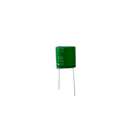
Supercapacitor — values that change constantly
Fit a supercapacitor to the +5 V pole and the internal 5 V stays up for about ten seconds after the main supply is cut. Wire the main supply into a digital input as well, add a rung that moves the live value into the retentive memory the moment that input goes off, and a second rung that moves it back once on restart. The EEPROM is then written only at the instant of a blackout, so it survives more than 100,000 of them.
Mounting · DIN railDIN Rail
Clips onto a 35 mm DIN rail, or screws down through the PCB's own holes
Inside a control panel the board clips onto a 35 mm DIN rail; built into a machine it screws down through the Ø3.5 mounting holes in the PCB. The board measures 160.0 × 100.0 mm without the rail clip, and stands 114.2 mm high once the clip is closed on the rail.
35 mm DIN rail
Clips onto the rail in a control panel
Direct PCB mounting
Screws through the Ø3.5 mounting holes
160.0 × 100.0 mm
PCB outline with no rail clip fitted
114.2 mm engaged
119.4 mm with the clip open, 114.2 mm closed
Mounting and dimensions
| Mounting | 35 mm DIN rail, or direct to PCB (Ø3.5 holes) |
|---|---|
| DIN rail | 35 mm |
| PCB alone (no clip) | 160.0 × 100.0 mm |
| Mounting holes | Ø3.5 mm · 143.2 × 90.0 mm apart |
| Clip open (before engaging) | approx. 119.4 mm |
| Clip closed (engaged) | approx. 114.2 mm |
Where no DIN rail is used, the board screws down through the Ø3.5 mounting holes in the PCB; on a rail, the clip closes over a 35 mm profile and the assembly stands 114.2 mm high.
Mounting on a 35 mm DIN rail
* The clip hooks over a 35 mm DIN rail. Overall height is 119.4 mm with the clip open and 114.2 mm once it is closed and engaged. The drawing shows the mounting method rather than the clip's own shape.
Outline and mounting holes
* The outline and mounting holes with no rail clip fitted. All dimensions in millimetres.
Installation notes
- Indoor use only. Do not install where there is rain, dust, frost, direct sunlight or condensation.
- Do not install in an atmosphere containing flammable or explosive gas.
- Do not install where there is heavy vibration or shock.
- Where the equipment affects life or property (nuclear, medical, marine, vehicle, aviation and the like), a secondary safety device must be fitted.
FAQ
How many I/O points does the MPS-16A8R8T have?▾
The MPS-16A8R8T provides 16 isolated digital inputs and 16 relay outputs, with onboard RS-485, RS-232, UART, I²C communication. See the specification table for the full breakdown.
Does the MPS-16A8R8T support Modbus RTU?▾
Yes. The MPS-16A8R8T supports Modbus RTU — master and slave alike — over its serial interface.


